


Lock Loop Clock Driver
A Lock Loop Clock Driver, also known as a PLL (Phase-Locked Loop) Clock Driver, is an electronic circuit that is used to generate a high-frequency clock signal with low jitter and drift. It is commonly used in digital systems to control timing and synchronization of circuits.
The basic principle of a PLL Clock Driver is that it compares the phase and frequency of an input signal with that of a synchronized output signal and adjusts the output signal to match the input signal. By doing so, the output signal can be locked to the input signal, resulting in a stable and precise clock signal.
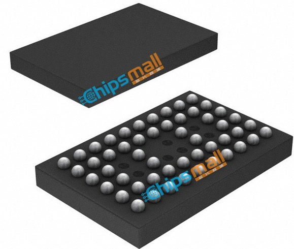
CDCUA877ZQLR Description
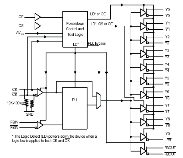
Made by Texas, The CDCUA877 is a high-performance, low-jitter, low-skew, zero-delay buffer that distributes a differential clock input pair (CK, CK) to ten differential pairs of clock outputs (Yn, Yn) and to one differential pair of feedback clock outputs (FBOUT, FBOUT). The clock outputs are controlled by the input clocks (CK, CK), the feedback clocks (FBIN, FBIN), the LVCMOS control pins (OE, OS), and the analog power input (AVDD). When OE is low, the clock outputs, except FBOUT/FBOUT, are disabled while the internal PLL continues to maintain its locked-in
frequency. OS (output select) is a program pin that must be tied to GND or VDD.
When OS is high, OE functions as previously described. When OS and OE are both low, OE has no affect on Y7/Y7, they are free running. When AVDD is grounded, the PLL is turned off and bypassed for test purposes.
When both clock inputs (CK, CK) are logic low, the device enters in a low power mode. An input logic detection circuit on the differential inputs, independent from input buffers, detects the logic low level and performs in a low power state where all outputs, the feedback, and the PLL are off. When the clock inputs transition from being logic low to being differential signals, the PLL turns back on, the inputs and the outputs are enabled, and the PLL obtains phase lock between the feedback clock pair (FBIN, FBIN) and the clock input pair (CK, CK) within the specified stabilization time.
The CDCUA877 is able to track spread spectrum clocking (SSC) for reduced EMI. This device operates from –40°C to 85°C.
CDCUA877ZQLR Logic Diagram
CDCUA877ZQLR Features
1.8-V/1.9-V Phase Lock Loop Clock Driver for Double Data Rate (DDR II) Applications
Spread Spectrum Clock Compatible
Operating Frequency: 125 MHz to 410 MHz
Application Frequency: 160 MHz to 410 MHz
Low Current Consumption: <200 mA Typ
Low Jitter (Cycle-Cycle): ±40 ps
Low Output Skew: 35 ps
Stabilization Time <6 μ
Distributes One Differential Clock Input to Ten Differential Outputs
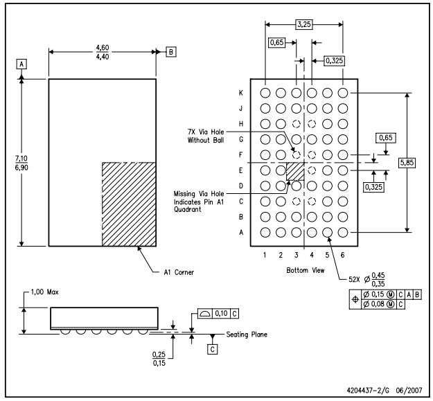
52-Ball μBGA (MicroStar Junior™ BGA, 0,65-mm pitch)
External Feedback Pins (FBIN, FBIN) are Used to Synchronize the Outputs to the Input Clockst
Meets or Exceeds CUA877/CAU878 Specification PLL Standard for PC2-3200/4300/5300/6400o
Fail-Safe Inputs
CDCUA877ZQLR Mechanical Data
CDCUA877ZQLR Product Parameter
|
Manufacturer |
Texas |
Manufacturer's Part # |
CDCUA877ZQLR |
|
Categories |
Integrated Circuits (ICs) |
Sub-Categories |
Clock/Timing - Application Specific |
|
Part Status |
Active |
PLL |
Yes |
|
Main Purpose |
Memory, DDR2 |
Input |
SSTL-18 |
|
Output |
SSTL-18 |
Number of Circuits |
1 |
|
Ratio - Input:Output |
1:10 |
Differential - Input:Output |
Yes/Yes |
|
Frequency - Max |
410MHz |
Voltage - Supply |
1.7V~1.9V |
|
Operating Temperature |
-40°C~85°C |
Mounting Type |
Surface Mount |
|
Package / Case |
52-VFBGA |
Supplier Device Package |
52-BGA MICROSTAR JUNIOR (7x4.5) |
|
Factory Lead Time |
6 Weeks |
Lifecycle Status |
ACTIVE (Last Updated: 1 week ago) |
|
Contact Plating |
Copper, Silver, Tin |
Mount |
Surface Mount |
|
Number of Pins |
52 |
Weight |
57.804678mg |
|
Packaging |
Tape & Reel (TR) |
Pbfree Code |
yes |
|
Number of Terminations |
52 |
Packing Method |
TR |
|
Terminal Position |
BOTTOM |
Terminal Form |
BALL |
|
Peak Reflow Temperature (Cel) |
260 |
Number of Functions |
1 |
|
Supply Voltage |
1.8V |
Terminal Pitch |
0.65mm |
|
Frequency |
410MHz |
Base Part Number |
CDCUA877 |
|
Pin Count |
52 |
Number of Outputs |
10 |
|
Operating Supply Voltage |
1.8V |
Nominal Supply Current |
225mA |
|
Family |
877 |
Max I(ol) |
0.009 A |
|
Height |
1mm |
Length |
7mm |
|
Width |
4.5mm |
Thickness |
750μm |
|
Radiation Hardening |
No |
RoHS Status |
ROHS3 Compliant |
|
Lead Free |
Lead Free |
Terminal Finish |
Tin/Silver/Copper (Sn/Ag/Cu) |
|
Logic IC Type |
PLL BASED CLOCK DRIVER |
Same Edge Skew-Max (tskwd) |
0.035 ns |
|
Output Characteristics |
3-STATE |
Subcategory |
Clock Drivers |
|
Technology |
CMOS |
|
|
CDCUA877ZQLR Manufacturer
Texas Instruments is a semiconductor multinational company in Texas, USA. It is famous for developing, manufacturing, and selling semiconductor and computer technology. It is mainly engaged in innovative digital signal processing and analog circuits. In addition to the semiconductor business, it also provides solutions including sensing and control, educational products and digital light source processing. Texas Instruments (TI) is headquartered in Dallas, Texas, USA, and has manufacturing, design or sales organizations in more than 25 countries.


